
HDI printed circuit board improve heat dissipation
A typical printed circuit board (PCB) contains many components that generate heat and require effective heat dissipation. If this is not done properly, it may lead to the failure of the PCB or other malfunctions in the device that it is installed in. HDI technology is one of the most advanced ways to improve heat dissipation and has become a popular option for reducing the size of PCBs.
An HDI printed circuit board is a high-density interconnect board that has been developed to allow more connections in a smaller space. This is achieved by using a multi-layer construction and microvia drilling techniques. The board is then fabricated using a sequential lamination process. The resulting boards can be very compact and offer superior performance.
The core of an hdi printed circuit board is made up of multiple insulating layers and copper foil. The insulating layers are laminated to the copper with a material called prepreg. The board is then drilled with small holes, either mechanically or by laser, to create the necessary interconnects between the layers of the PCB. The holes are then filled with an electroplated metal like gold or silver to make them electrically conductive. These holes are known as vias and they can be located in different places in the PCB, depending on the design requirements.
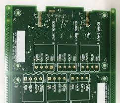
How does an HDI printed circuit board improve heat dissipation?
Using microvias, the number of layers in an HDI PCB can be reduced without sacrificing connectivity. They also have a smaller diameter than through-holes, which allows them to be placed more closely together. These features contribute to the lower operating temperatures of HDI PCBs compared to standard ones.
To further improve heat dissipation, the components in an HDI PCB are arranged according to their heat generation and thermal pathways. The heat-generating components are positioned closer to the airflow vents to help minimize hot spots and ensure that heat disperses evenly throughout the PCB. In addition, thermal pads are used to improve the conductivity of the component connections and increase the surface area for heat dissipation.
Lastly, the HDI PCB design is optimized to reduce the length of the signal paths and improve the signal integrity of the devices that are installed in the board. This is achieved by placing the components close to each other so that they don’t have to travel long distances for data transmission.
As the demand for smaller gadgets increases, there is an increased need for technologies that can help reduce their size. HDI is a very important advancement in this field and is being utilized in various applications including aerospace and military equipment. Its robustness and compact structure makes it well-suited to extreme conditions and physical impacts. This makes it a great choice for use in avionics, smart weapons, and defense networks. HDI is also being deployed in industrial automation to streamline and optimize processes. The compactness of HDI PCBs makes them a great choice for these types of environments. Sierra Circuits is a leading manufacturer of HDI PCBs and has the expertise and experience needed to provide customers with turnkey PCB assemblies that will work as expected.