
Can printed circuit board assembly accommodate
Printed Circuit Board Assembly (PCBA) has evolved significantly over the years to meet the growing demands for smaller, more powerful electronic devices. One of the key advancements in PCB technology is the ability to accommodate high-density interconnects (HDIs), which enable designers to pack more functionality into smaller form factors. But can Printed Circuit Board Assembly truly accommodate high-density interconnects, and what are the implications for electronic device design and manufacturing?
High-density interconnects (HDIs) refer to advanced PCB designs that incorporate densely packed components, fine-pitch traces, and multiple layers to achieve higher signal density and routing efficiency. HDIs are characterized by features such as microvias, blind vias, and buried vias, which allow for tighter component spacing and more efficient signal routing between layers. These features enable designers to create PCBs with higher component density, reduced signal propagation delays, and improved electrical performance.
printed circuit board assembly can indeed accommodate high-density interconnects, but it requires specialized manufacturing techniques and processes to realize the full potential of HDI technology. Advanced PCB fabrication methods such as laser drilling, sequential lamination, and controlled-depth drilling are used to create the intricate layer stack-ups and complex interconnects required for HDI designs. Additionally, advanced assembly techniques such as fine-pitch surface mount technology (SMT) and automated optical inspection (AOI) are employed to mount and inspect components with precision and accuracy.
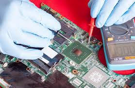
Can printed circuit board assembly accommodate high-density interconnects?
The adoption of HDI technology in Printed Circuit Board Assembly offers several benefits for electronic device design and manufacturing. One of the primary advantages is the ability to create smaller and more compact electronic devices without sacrificing functionality or performance. By reducing the size of the PCB footprint and increasing component density, designers can develop sleeker, more portable devices that meet the demands of today’s mobile and wearable technology markets.
Furthermore, HDI technology enables designers to overcome the limitations of traditional PCB designs, such as signal integrity issues, electromagnetic interference (EMI), and thermal management challenges. By utilizing microvias and other advanced interconnect techniques, designers can achieve shorter signal paths, reduced crosstalk, and improved impedance control, resulting in higher-speed, more reliable electronic systems.
Another significant advantage of HDI technology in Printed Circuit Board Assembly is the potential for cost savings and manufacturing efficiencies. While HDI PCBs may have higher upfront costs due to the complexity of fabrication and assembly, they can often lead to overall cost savings by reducing the number of PCB layers, minimizing material waste, and streamlining production processes. Additionally, the smaller size and weight of HDI PCBs can result in lower shipping and handling costs, further contributing to cost savings over the product lifecycle.
In conclusion, Printed Circuit Board Assembly can indeed accommodate high-density interconnects, offering designers and manufacturers the flexibility to create smaller, more powerful electronic devices with improved performance and reliability. The adoption of HDI technology in PCB manufacturing opens up new possibilities for innovation and differentiation in electronic device design, enabling the development of next-generation products that meet the evolving needs of consumers and industries. As technology continues to advance, the role of HDI technology in Printed Circuit Board Assembly will only become more pronounced, driving further advancements in electronic device design and manufacturing.