
3D printer for PCB prototypes
Using a 3D printer for PCB prototypes is a topic that has gained significant attention in recent years. While traditional methods of PCB manufacturing, such as etching and milling, remain the standard for creating high-performance and precise prototypes, 3D printing offers an alternative for certain applications, especially when rapid prototyping and flexibility are needed. The question of whether a 3D printer can be used for PCB prototypes hinges on understanding the capabilities of 3D printing technology and the specific requirements of the PCB prototype.
A key factor in using a 3D printer for PCB prototypes is the ability to quickly produce physical models for testing and validation. 3D printers can be used to create the physical layout of the pcb prototype, allowing designers to quickly test the form factor and component placement before committing to traditional manufacturing processes. For simple, low-complexity designs, 3D printing can be an effective method for producing prototypes in a fraction of the time it would take using conventional methods. This is particularly useful for validating the size and shape of the board, checking for potential interference with other components, or visualizing the design in 3D.
However, when it comes to the electrical functionality of the PCB prototype, traditional 3D printing faces limitations. Standard 3D printers typically use plastic filaments, such as PLA, ABS, or PETG, which are not conductive and cannot be used to create the electrical traces or pads that are essential for PCB functionality. While there are some advanced 3D printers capable of printing conductive materials, such as conductive inks or pastes, these printers are still relatively rare and are typically more expensive. Even with the ability to print conductive materials, achieving the level of precision required for creating reliable electrical connections and maintaining signal integrity can be challenging.
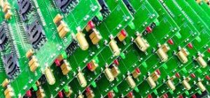
Can I use a 3D printer for PCB prototypes?
For most applications, 3D printing is better suited for creating the mechanical structure of the PCB prototype, rather than the electrical components. A 3D printer can be used to fabricate the base structure of the PCB, including the board itself and mounting points for components. This approach can be helpful when designing prototypes for enclosures, connectors, or housings for electronic devices. In such cases, 3D printing can allow for quick adjustments to the design, especially for testing different form factors or configurations without the need for expensive tooling or equipment.
In some cases, hybrid approaches are used, where a 3D printer is employed to create the mechanical parts of the PCB prototype, while the electrical traces and components are added through traditional PCB manufacturing techniques. This can provide a cost-effective solution for rapid prototyping, especially when testing a new product or making iterative changes. By combining 3D printing with conventional PCB manufacturing, designers can accelerate the prototyping process and minimize the costs associated with producing multiple iterations.
Despite these limitations, 3D printing for PCB prototypes continues to evolve, and new technologies are emerging that could expand the potential applications. Researchers and companies are experimenting with conductive inks and materials to enable 3D printers to fabricate fully functional PCBs, but this technology is still in the experimental stages and is not yet widely available for mass production. For now, 3D printing can be an excellent tool for creating prototype enclosures, mechanical structures, and form factors but is not yet a fully viable solution for producing high-performance, electrically functional PCB prototypes.
In conclusion, while 3D printers are not yet able to fully replace traditional PCB manufacturing techniques for electrically functional prototypes, they can still be a valuable tool for specific aspects of the PCB prototype development process. 3D printing can be used to quickly create the physical layout and form factor of a PCB, making it easier to test designs and iterate quickly. For the electrical functionality of a PCB prototype, however, traditional manufacturing methods remain the best option.